
Compétences technologiques
RENATECH s’appuie sur l’expertise et les équipements de pointe de ses 5 laboratoires répartis sur le territoire français pour répondre à un large éventail de besoins technologiques transversaux ou spécifiques.
CROISSANCE DE MATÉRIAUX
MBE/MOCVD . UHV-CVD . Synthèse chimique . ALD . Procédés thermiques . Implantation d’ions
CARACTÉRISATION / MÉTROLOGIE
Microscope optique . AFM/STM/SEM/TEM . Profilométrie . Ellipsométrie . Mesures électriques et optiques . Diffraction rayons X
DÉPÔT
PVD (évaporation/pulvérisation) . PECVD/LPCVD . Dépôt électrochimiques . Technologies alternatives (jet d’encre, sérigraphie)
LITHOGRAPHIE
Faisceaux d’électrons . UV et extrême UV . Laser . Nano-impression
GRAVURE
Chimique . Plasma . Laser . FIB, nanoFIB
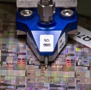
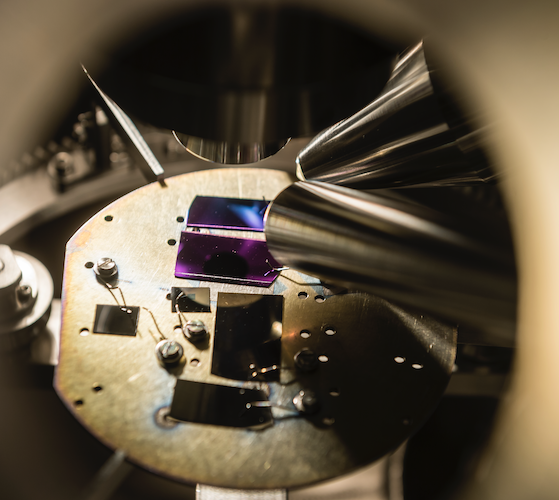
INTEGRATION
Packaging de puces . Rectification . Pick and place . Câblage par fil . Packaging pleine plaque . Soudure de tranches . Sérigraphie