
Saclay
![]()
Salle blanche : 2900 m² (ISO 4 à 7)
Thèmes recherche principaux : silicium pour la nanophotonique, spintronique, dispositifs optoélectroniques, microsystèmes, nanophotonique III-V, nano-électronique quantique, dispositifs optoélectroniques, microfluidique
Staff technique : 40 techniciens/ingénieurs
Équipements spécifiques : IV-IV epitaxy, Magnetic thin layers, E-Beam lithography, Deep-UV lithography, Direct laser writing, ICP deep etching of silicon, Optical vibrometry, III-V epitaxy (MBE, MOCVD), E-Beam lithography tools, III-V deep etching, NanoFIB, AFM/STM, nanoimprint lithography tools, STEM with correction of aberration, 3D lithography, Xray analysis
Adresse :
10 Boulevard Thomas Gobert
91120 Palaiseau, France
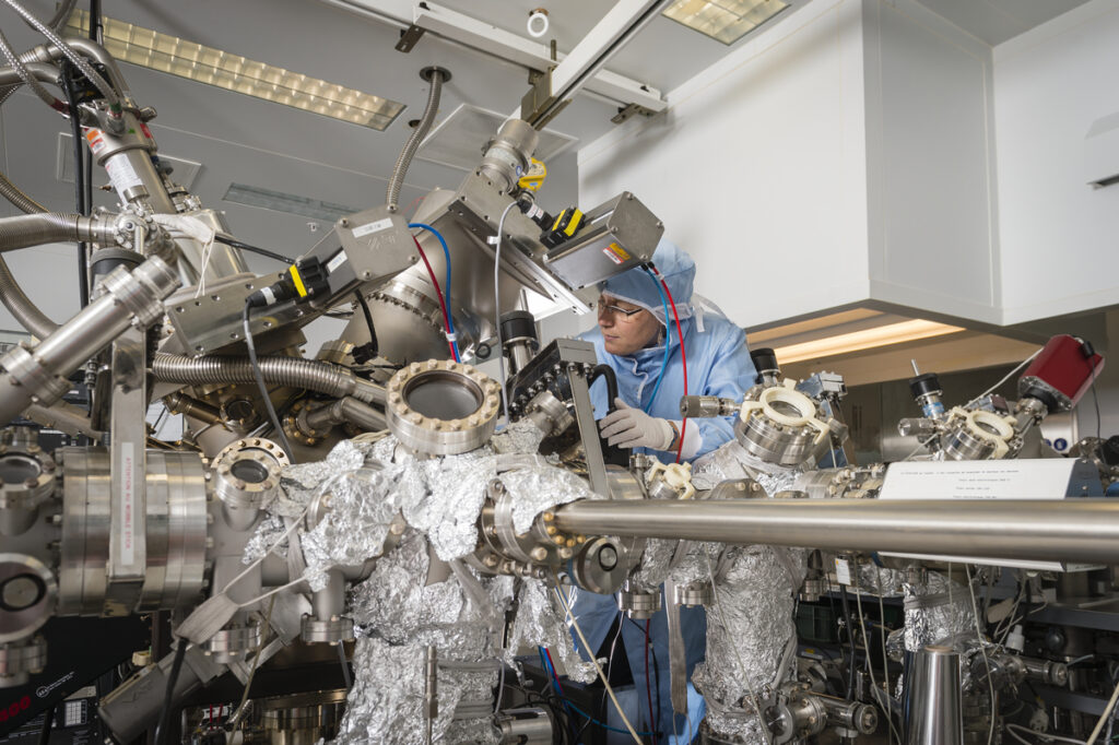
Lille
Salle blanche : 1 600 m² (ISO 5 à 7)
Thèmes de recherche principaux :
électronique (III/V, Si, souple, 2D, puissance), nanocaractérisation, photonique THz, MEMS-NEMS-BIOMEMS, Dispositifs pour l’énergie
Staff technique : 26 techniciens/ingénieurs
Équipements spécifiques :
Lithographie (e-beam, Laser, UV), Soft lithographie, PVD, PECVD, LPCVD, ALD, RIE, ICP, DRIE, épitaxie III/V, Implantation Ionique, FIB, AFM/STM, STM 4 pointes, L2, Ablation laser, Packaging
Adresse :
Cité Scientifique
avenue Poincaré BP 60069
59652 Villeneuve d’Ascq Cedex
Contact : accueil-projets@iemn.fr
Toulouse
![]()
Salle blanche : 1 600 m² (ISO 4 à 6)
Thèmes de recherche principaux : intégration de systèmes : RF, énergie photonique, micro et nanosystèmes pour la biologie, santé et environnement
Staff technique : 30 techniciens/ingénieurs
Équipements spécifiques : Lithography (E-beam, Laser 2D, 3D , UV par projection, FLICE, bi-photons), PVD, Dépôts électrolytiques, PECVD, LPCVD, ALD, DRIE, implantation ionique, FIB, Jet d’encre, Packaging.
Adresse :
7, avenue du Colonel Roche
BP 54200
31031 Toulouse Cedex 4
Grenoble
![]()
Salle blanche : 1 200 m² (ISO 4 à 6)
Thèmes de recherche principaux : opto et nano-électronique, spintronique, photonique, nanosystèmes pour la Santé, l’Environnement et l’Energie
Staff technique : 30 techniciens/ingénieurs
Plateformes technologiques :
- GECCO 200-300 : Procédés avancés compatibles 300 mm (MOCVD, gravure par plasma, XPS quasi-in situ, Raman, FIB-SEM…)
- PTA : Procédés génériques pour la réalisation d’un composant jusqu’à 100 mm (lithographie électronique, optique, gravure et dépôt, packaging…)
- CAMELEON : Procédés exploratoires et prototypage (Caractérisation thermique, électrique, physico-chimique et de surface, lithographie UV et laser 3D, PVD…)
Adresse :
Laboratoire des Technologies de la Micro-électronique, UMR5129
c/o CEA-Leti Minatec
17 avenue des Martyrs
38054 Grenoble cedex 9
Contact :
camille.petit-etienne@cea.fr
Besançon
![]()
Salle blanche : 865 m² (ISO 5 à 7)
Thèmes de recherche principaux : Micro- et nano-acoustique, micro-nano-optique, microrobotique, sillicium, MOEMS
Staff technique : 12 techniciens/ingénieurs
Équipements spécifiques : AIN deposition, E-Beam lithography, Spray coating, Dry plasma etching (Si, quartz, LINbO3),FIB,
Wafer bonding, Precision dicing, Mechanical characterization, Industrial production line for plezoelectric components.
Adresse :
Centrale de Technologie
MIMENTO TEMIS-Innovation
Maison des Microtechniques
18 rue Alain Savary
25000 Besançon
Contact : mimento@femto-st.fr